


Atomic Layer Deposition Equipment Market Size, Share, Competitive Analysis & Forecast 2034
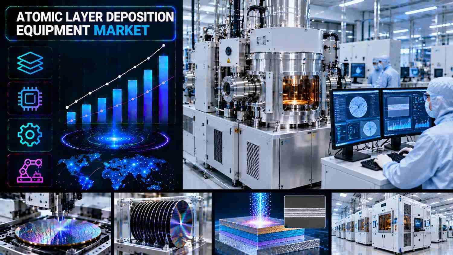
IMARC Group, a leading global market research and management consulting firm, has published its latest market intelligence report on the atomic layer deposition equipment market. The global atomic layer deposition equipment market grew from USD 8.5 Billion in 2025 to USD 9.9 Billion in 2026. The market is projected to reach USD 26.1 Billion by 2034, exhibiting a CAGR of 12.83% from 2026-2034. The market is witnessing steady expansion, driven by rising demand for advanced semiconductors at sub-5nm nodes, rapid growth in 3D NAND and DRAM memory architectures, increasing adoption of GAAFET and FinFET transistor designs, and expanding use of thin-film coatings in solar cells, flexible displays, batteries, and medical devices worldwide.
The industry is experiencing strong growth momentum because atomic layer deposition (ALD) is one of the few processes able to build films one atomic layer at a time with near-perfect uniformity. As chip features shrink and structures grow taller, conventional deposition methods struggle to coat deep trenches and high-aspect-ratio 3D structures evenly. ALD equipment fills this gap with precise, conformal films for high-k dielectrics, metal gates, spacers, liners, and barrier layers. Demand from AI accelerators, 5G devices, and power-efficient consumer electronics is reinforcing the need for these tools. At the same time, ALD is moving beyond the fab into flexible OLED encapsulation, lithium-ion battery coatings, MEMS devices, and biocompatible medical coatings.
How AI is Reshaping the Future of the Atomic Layer Deposition Equipment Market
-
AI Chip Demand Driving Advanced Node Deposition Needs: Training and inference processors for AI data centers rely on gate-all-around transistors and high-bandwidth memory stacks, both of which depend on ALD for ultra-thin, defect-free films. This is pulling equipment orders toward more advanced, multi-chamber platforms.
-
Machine Learning for Process Control and Yield Optimization: Fabs are applying AI-based analytics to chamber sensor data, precursor delivery, and film thickness metrology. This helps detect drift early, shorten recipe development, and keep atomic-scale uniformity consistent across thousands of wafers.
-
AI-Assisted Materials Discovery for New Precursors: Computational models are accelerating the screening of new precursor chemistries and low-temperature processes. This supports next-generation materials such as molybdenum and other low-resistance metals that ALD tools must deposit reliably at volume.
Grab a sample PDF of this report: https://www.imarcgroup.com/atomic-layer-deposition-equipment-market/requestsample
Atomic Layer Deposition Equipment Market Trends and Drivers
The global atomic layer deposition equipment market is expanding on the back of semiconductor scaling, memory architecture changes, and a widening set of non-semiconductor applications. Chipmakers moving to sub-5nm nodes need films only a few atoms thick that wrap uniformly around complex 3D transistor structures. ALD is the process of choice for this, which makes the equipment a structural requirement rather than an optional upgrade at leading-edge fabs.
Memory is a second major demand engine. In 3D NAND, manufacturers stack well over a hundred layers and etch extremely deep channels that must be coated uniformly from top to bottom. In DRAM, ALD supports capacitor dielectrics and barrier layers as cell dimensions keep shrinking. A single advanced logic or memory fab uses ALD tools across dozens of process steps, so each new fab built means a large batch of equipment orders.
Government support is amplifying this demand. The United States CHIPS and Science Act earmarked roughly USD 52 Billion for domestic semiconductor manufacturing and research. The EU Chips Act mobilizes public and private funding to strengthen semiconductor sovereignty across the bloc. India's Semiconductor Mission offers fiscal support of up to half of project costs for fabs and packaging units. China's Big Fund III, announced in May, raised about RMB 344 Billion to back its domestic chip supply chain. Each program adds to the pipeline of cleanrooms that will need deposition tools.
New application areas are also opening up. Flexible OLED displays use ALD barrier films to block moisture and oxygen. Solar manufacturers apply aluminum oxide passivation layers to lift cell efficiency. Battery developers use ultra-thin coatings on electrode particles to improve cycle life and stability. Emerging fields such as quantum computing, photonics, wearables, and environmental sensors are creating further room for modular, customizable ALD platforms.
Atomic Layer Deposition Equipment Industry Segmentation
The report has segmented the market into the following categories:
Breakup By Product:
- Metal ALD
- Aluminum Oxide ALD
- Plasma Enhanced ALD
- Catalytic ALD
- Others
Aluminum oxide ALD accounts for the largest product share at 37.9%. Its leadership reflects the material's strong dielectric strength, chemical stability, and excellent barrier performance, which suit gate dielectrics, passivation layers, and encapsulation films across semiconductors, solar cells, and flexible displays. Plasma enhanced ALD is gaining ground where lower process temperatures and wider material choices are required.
Breakup By Application:
- Semiconductors
- Solar Devices
- Electronics
- Medical Equipment
- Others
Semiconductors hold the largest application share at 46.7%. Logic, DRAM, and 3D NAND production all depend on ALD for high-k dielectrics, metal gates, spacers, and barrier layers, and this reliance deepens with every move to smaller nodes and 3D transistor structures.
Breakup By Region:
- North America (United States, Canada)
- Asia Pacific (China, Japan, India, South Korea, Australia, Indonesia, Others)
- Europe (Germany, France, United Kingdom, Italy, Spain, Russia, Others)
- Latin America (Brazil, Mexico, Others)
- Middle East and Africa
Asia Pacific dominates the global atomic layer deposition equipment market with a commanding 73.8% share. The region hosts the world's densest cluster of foundries and memory makers across China, South Korea, Taiwan, and Japan, and these facilities continuously invest in new deposition capacity. North America is growing steadily, led by the United States, as CHIPS Act projects move from announcement to construction. Europe is expanding through semiconductor sovereignty initiatives, including the EU Chips Act and a coalition of nine European countries formed in March to strengthen the regional chip ecosystem. Latin America and the Middle East and Africa are smaller but emerging markets, supported by research investment, renewable energy projects, and Gulf semiconductor ambitions.
Competitive Landscape
The report provides a comprehensive analysis of the competitive landscape in the atomic layer deposition equipment market with detailed profiles of all major companies, including:
- ANRIC Technologies
- Applied Materials
- Arradiance
- ASM International
- Beneq
- Forge Nano
- Lam Research
- NCD Co.
- Oxford Instruments
- SENTECH Instruments
- The Kurt J. Lesker Company
- Tokyo Electron
- Veeco Instruments
The market is moderately consolidated, with a few dominant global suppliers alongside a growing number of niche entrants focused on specialized, research-grade, and roll-to-roll systems.
What Does The Full Report Cover?
If you are tracking the atomic layer deposition equipment market for investment decisions, market entry planning, competitive benchmarking, or strategic advisory, IMARC Group's full atomic layer deposition equipment market report gives you everything in one place:
- Complete market sizing with detailed projections across the full study period
- Quantified growth driver analysis across product, application, and regional markets
- Sub-segment breakdowns for metal, aluminum oxide, plasma enhanced, and catalytic ALD, with individual share data
- Country-level data for the United States, Canada, Germany, France, the United Kingdom, Italy, Spain, Russia, China, Japan, India, South Korea, Australia, Indonesia, Brazil, and Mexico
- Competitive profiles of 13 leading companies with strategic landscape assessment
- Porter's Five Forces, value chain analysis, and pricing intelligence
- Latest innovation trends in 3D NAND and DRAM deposition, GAAFET architectures, flexible electronics, and modular ALD platforms
Recent News and Developments in Atomic Layer Deposition Equipment Market
-
February: Lam Research launched ALTUS Halo, a tool designed for high-volume molybdenum deposition. The platform targets advanced logic and memory makers seeking lower-resistance metallization as feature sizes shrink.
-
January: Forge Nano opened a new cleanroom to triple production capacity of its TEPHRA tools. The expansion strengthens its supply of compact ALD systems for research labs and pilot lines.
-
November: 2D Generation ordered an ALD machine from Beneq for developing graphene-coated interconnects. The order highlights ALD's growing role in next-generation interconnect materials.
-
October: AIM Photonics received USD 321 million to support U.S. silicon photonics manufacturing. In the same month, Samsung and TSMC began talks with the UAE on chip plants, signaling new regional demand for fab equipment.
-
August: Kalpana Systems introduced roll-to-roll spatial ALD tools for solar, OLED, battery, and packaging applications, bringing high-throughput atomic-scale coatings to large-area products.
-
July: Chipmetrics launched test chips for ALD process monitoring, while Forge Nano introduced its TEPHRA cluster tool for 200mm wafers, widening access to ALD for mature-node and specialty device makers.
Note: If you require specific details, data, or insights that are not currently included in the scope of this report, we are happy to accommodate your request. As part of our customization service, we will gather and provide the additional information you need, tailored to your specific requirements.
Key Questions This Report Answers
- What is the current global atomic layer deposition equipment market size?
- Which product segment holds the largest share in the global atomic layer deposition equipment market?
- Which application drives the most demand for ALD equipment?
- What are the key drivers of global atomic layer deposition equipment market growth?
- Which region dominates the global atomic layer deposition equipment market and why?
- How are 3D NAND, DRAM, and GAAFET architectures reshaping equipment requirements?
- Who are the top companies in the global atomic layer deposition equipment market and what are their competitive strategies?
- What are the investment and market entry opportunities across quantum computing, photonics, wearables, and flexible electronics?
About Us
IMARC Group is a global management consulting firm that helps the world's most ambitious changemakers to create a lasting impact. The company provides a comprehensive suite of market entry and expansion services. IMARC offerings include thorough market assessment, feasibility studies, company incorporation assistance, factory setup support, regulatory approvals and licensing navigation, branding, marketing and sales strategies, competitive landscape and benchmarking analyses, pricing and cost research, and procurement research.
Media and Sales Contact
IMARC Group
Email: sales@imarcgroup.com
United States: +1-201-971-6302
India: +91-120-433-0800
United Kingdom: +44-753-714-6104

 English
 Arabic
 French
 Spanish
 Portuguese
 Deutsch
 Turkish
 Dutch
Dutch
 Italiano
 Russian
 Portuguese (Brazil)
 Greek
Greek
 Bengali